Reading...
![]()
Play button
![]()
Play button
![]()
Use LEFT and RIGHT arrow keys to navigate between flashcards;
Use UP and DOWN arrow keys to flip the card;
H to show hint;
A reads text to speech;
4 Cards in this Set
- Front
- Back
- 3rd side (hint)
|
Define Band Energy Gaps
|
1. Energy Gap between the Valence bonds and Conduction bonds is known as Band Energy Gap
2. It is "0"ev for metallic conductors, less than "3'ev for semi conductors and greater than "3"ev for insulators [e,v - electron volts] |
|
|
|
Define Valence Band and Conduction Band
|
1. Electrons inside a crystal have different energy levels.
2. The different energy levels with continuous energy variation is called energy band 3. The energy band which includes the energy levels of valence electrons is called "valence bonds" 4. The bond with energy levels higher than valence electrons is called "conduction bond" |
|
|
|
Fermi Level
|
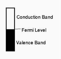
Fermi Level is essentially the level half way between Conduction Band and Valence Band
|
Fermi Level is essentially the level half way between Conduction Band and Valence Band
|
|
|
Chapter 14 - Page 509 - Q - 14.1
In an n-type silicon, which of the following statement is true: (a) Elect rons are major i ty car r iers and t r ivalent atoms are the dopants. (b) Electrons are minority carriers and pentavalent atoms are the dopants. (c) Holes are minor i ty car r iers and pentavalent atoms are the dopants. (d) Holes are majority carriers and trivalent atoms are the dopants |
uuu
|
|